HDI PCB
HDI PCB
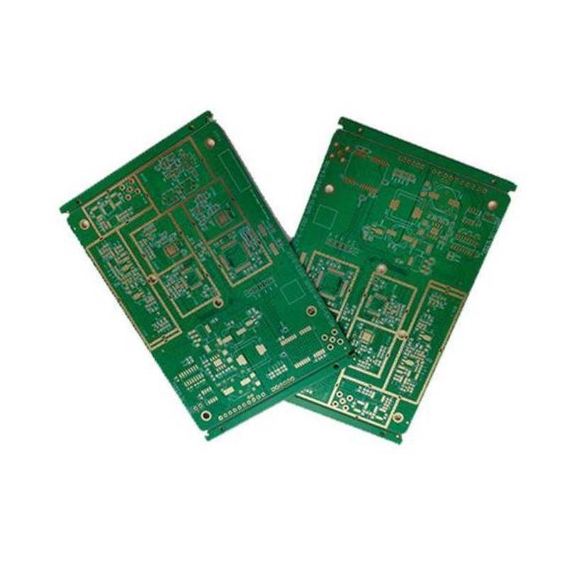
High-Density Interconnect (HDI) PCBs represent one of the most advanced categories of printed circuit boards. Unlike traditional boards, HDI PCBs feature a higher wiring density per unit area, achieved through finer lines and spaces, smaller vias, and higher connection pad density. They utilize technologies such as blind vias, buried vias, and microvias (typically laser-drilled) to maximize functional efficiency within a compact footprint.
High-Density Interconnect (HDI) PCBs represent one of the most advanced categories of printed circuit boards. Unlike traditional boards, HDI PCBs feature a higher wiring density per unit area, achieved through finer lines and spaces, smaller vias, and higher connection pad density. They utilize technologies such as blind vias, buried vias, and microvias (typically laser-drilled) to maximize functional efficiency within a compact footprint.
Key Features
• Microvias Technology: Utilizes laser-drilled microvias (often < 150µm) to enable direct interconnections between layers, significantly reducing signal reflection.
• High Circuit Density: Incorporates finer trace widths and spaces, allowing for more components to be mounted on both sides of the board.
• Advanced Via-in-Pad: Allows vias to be placed directly on component pads, improving signal integrity and saving space.
• Sequential Lamination: Employs a multi-layering build-up process that stacks layers sequentially rather than laminating all at once.
• Thin Material Layers: Often constructed with low-loss, thin dielectric materials to reduce overall weight and thickness.
Advantages
- Miniaturization: Reduces board size and weight by up to 60-70% compared to conventional PCBs, enabling sleeker product designs.
- Enhanced Electrical Performance: Shorter signal paths and lower power loss due to reduced capacitive and inductive effects.
- Improved Signal Integrity: Reduced stub length and impedance control ensure high-frequency signals are transmitted with minimal distortion.
- Superior Thermal Management: Dense copper circuitry and via-in-pad technology help dissipate heat more efficiently.
- Cost-Effective in System: While the board itself may be pricier, the overall system cost is often lower due to reduced layer counts, smaller connectors, and a minimized physical footprint.
- High Reliability: Better performance under thermal stress and vibration due to robust stacked via structures.
Application Scenarios
• Consumer Electronics: Smartphones, tablets, and laptops where space is at a premium and high-speed processing is required.
• Medical Devices: Hearing aids, pacemakers, and endoscopic cameras requiring ultra-miniature boards with zero margin for error.
• Automotive Electronics: ADAS (Advanced Driver-Assistance Systems), infotainment systems, and engine control units that must withstand harsh environments.
• Telecommunications: 5G base stations, RF antennas, and network servers demanding high-frequency transmission.
• Aerospace & Military: Avionics, radar systems, and portable communication devices where weight reduction and reliability are critical.
• Industrial Controls: High-precision sensors and robotic control units requiring dense component assembly.
Call to Action:
Ready to shrink your design without compromising performance? Contact us for a quote on your next HDI PCB project.